
PCB or Printed circuit board, a small green board, with markings, looks like the satellite view of locality, presents in nearly all electronic devices that compute. It acts as the heart of any computational electronic device by routing electrical signals through a copper pathway. Connecting all the components inside, PCB makes the device usable.
Types of PCB
When it comes to PCB manufacturing, there are 3 types of PCB – Single-sided PCB, Double-sided PCB and Multilayer PCB.
PCB Manufacturing
1. Designing
First step is to design it. The blueprint will be encoded with computer software to find out the errors in the design.
2. Printing
In the next step the design is printed only in a special printer called plotter printer in semi- transparent film like product – like photo negative.
3.nStructuring
Now, the board needs to be done first as it will give it a body. This is made of epoxy resin and glass fiber which are also called substrate material. And the copper is pre-bonded from the both side of the layer and cleaned to go to the next step. All these manufacturing steps are done mostly in pcb solutions fabrication houses.
4. Printing the inner layers
The laminated panel is covered by a photosensitive film called resist and exposed to ultraviolet light. This process helps to compare the blueprint and the actual prints through the holes.
Now the ultraviolet ray hardens the photoresist by revealing the copper pathway.
5. Removing the extra copper
In the next step is to get rid of the unwanted copper by washing the board with an alkaline solution.
6. Alignment inspection
Now, after lining up the inner and outer layer with help of the holes, an optical punch machine will punch a pin through the both layers. Another machine will inspect the final alignment.
7. Laminating
An epoxy resin layer will go on the alignment followed by a layer of the substrate. They a copper foil and more epoxy resin will go. One more copper layer will be applied as press plate. Then a mechanical press will be used to fuse all the layers together.
8. Drill
In PCB manufacturing process, after locating the drill spots by an x-ray machine, a computer-guided drill makes the holes to open the substrate and the inner panel. Additional copper is removed after completing this step.
9. Plating
Now, the plate is coated with a chemical to fuse all the layers together and cleaned with another set of chemicals. This process coats a copper layer on top and also it goes inside the holes.
10. Outer layer imaging
A coat of photoresist is applied on the outer layer. Ultra violet ray hardens the outer layer and removes any excess of it.
11. Plating
Again a copper layer is applied on the outer part of the panel. And then a thin layer will also be applied to protect the copper. By removal of unwanted copper the connection is established now.
12. Solder Mask Application
In the next step of PCB fabrication again the epoxy resin is coated before applying solder mask. Then it is baked with ultraviolet rays and removes all unwanted mask.
13. Silkscreening
In this process all the important information is printed on the panel and coated for the last time.
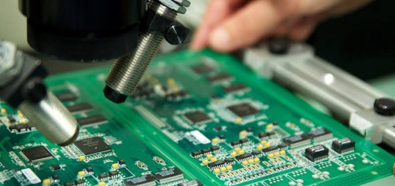
14. Testing
As a final step, a technician performs an electrical test to verify its functionality.
ChinaPCBOne Technology LTD. is author of this article on PCB manufacturing. Find more information about Field inspection solution.

